From Concept to Finished Product
End-to-end design for connected hardware. From first idea and working prototypes to a manufacturable, production-ready enclosure.
Insyght is a specialised IoT product development studio. We work with founders, corporate innovation teams, and hardware scale-ups who need to bring a connected product to market and need one team to handle the full stack.
Most IoT hardware projects follow the same fragmented path. A freelancer for the PCB. A separate agency for the enclosure. A software party for the app. Another for production in Asia. When something breaks (and it always does), nobody owns the problem. Timelines slip. Blame gets distributed. The product from the factory does not match the original vision.
We built Insyght because we have lived on both sides of that problem. Our team has worked on IoT products at scale, managed factories in Shenzhen, and seen what happens when hardware and software teams have never spoken to each other. We built an integrated studio specifically to eliminate that fragmentation.
What End-to-End Means
Concept validation
feasibility, BOM cost, connectivity choice
Electronics design
schematic, PCB layout, component selection, DFM
Embedded firmware
RTOS, drivers, application logic, power, OTA
Industrial design
enclosure, 3D CAD, prototyping, injection moulding
Mobile & web apps
React Native and React portals
IoT cloud backend
NodeJS, IoT Hub, telemetry, REST API
Parts sourcing
global supplier network procurement
Manufacturing
qualified factories in Shenzhen, QA on the ground
Certification
CE, FCC, UKCA, RoHS, accredited lab coordination
Insyght Console
OTA, fleet monitoring, factory quality logging
Electronics need a body. The board inside a connected product is invisible to the end user. What they see, touch, and judge is the industrial design. At Insyght, industrial design is not a bolt-on service: our designer, an iF Design Award winner, works inside the same team as the PCB engineers and firmware developers. The enclosure is designed knowing exactly what is inside it.
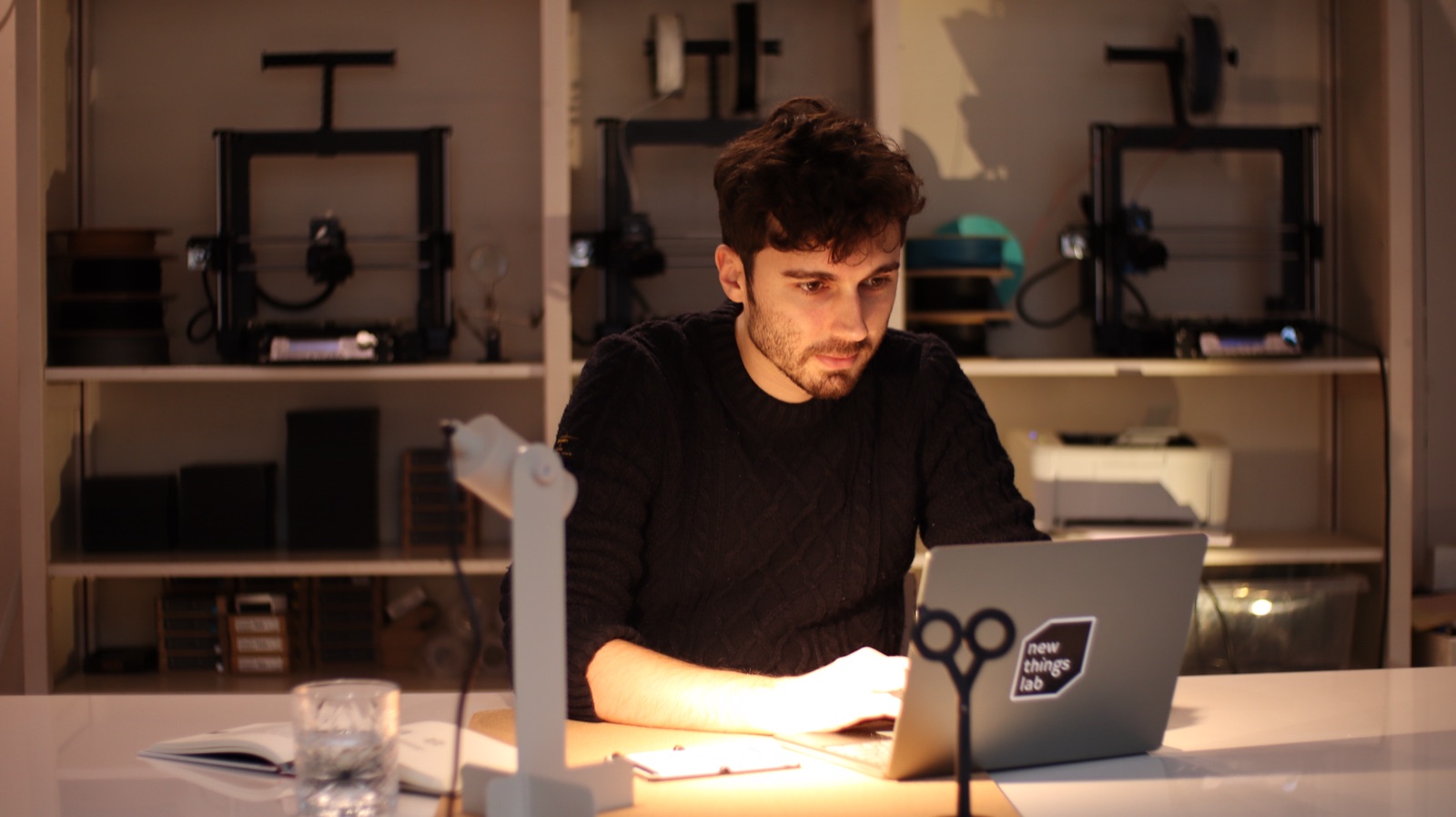
What Sets Our Industrial Design Apart
Most electronics design studios treat industrial design as a separate phase, something that happens after engineering is done. We do the opposite. Our industrial designer is in the product definition meeting, not the product handoff meeting.
Board dimensions are defined jointly with the enclosure concept, not retrofitted after layout
Connector placement, button locations, and indicator lights are designed around the enclosure, not worked around by it
Thermal management, IP sealing, and mechanical stress on components are considered before the first PCB is sent to production
The enclosure is optimised for injection moulding from the start, avoiding costly tooling modifications later
Our Capabilities
Concept Sketching
Rapid visual exploration of product directions
3D CAD Modelling
Fusion 360, production-ready part files
IP-Rated Enclosures
IP54 through IP68 sealing design
DFM
Snap fits, draft angles, wall thickness, parting lines
Rapid Prototyping
SLA/FDM/SLS prints for form and user testing
Injection Moulding Prep
Tool-ready CAD, material and finish specification
Surface Treatment
Texture, painting, pad printing, laser etching
Packaging Design
Retail-ready packaging concepts
From Sketch to Certified Product
Our industrial design process runs from rough concept sketches through to the 3D files that go to your injection moulding factory in Shenzhen. We manage the tooling process through our on-the-ground quality engineer in China, reviewing first-shot samples and coordinating modifications. When the mould is approved and the board is tested, you receive a finished product, not a set of files to hand to yet another supplier.
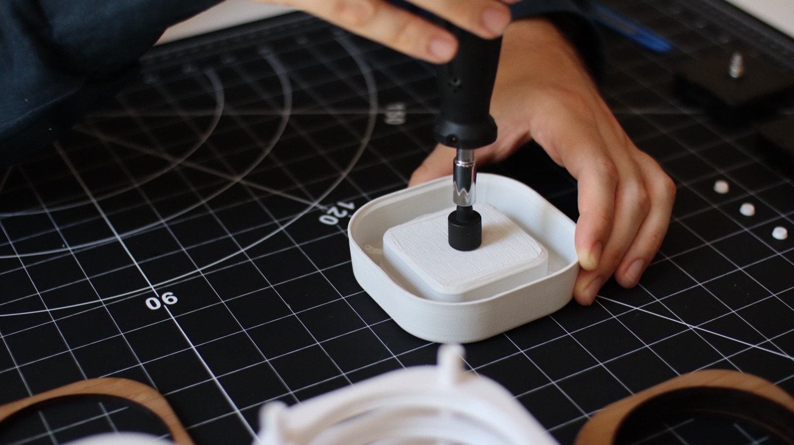
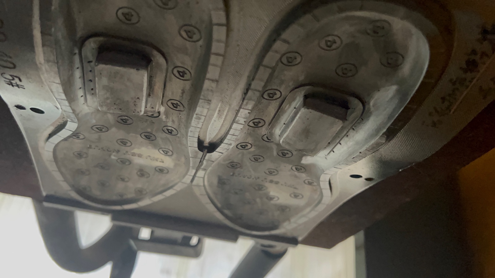
Award-Winning Design for Practical Products
Beautiful IoT hardware is not a luxury: it is a commercial requirement. B2B buyers judge products on aesthetics as much as specification sheets. Our iF Design Award winner brings international design rigour to every enclosure, alongside the pragmatism of someone who knows what a DFM report looks like.
One Team, From Concept to Production
Industrial design, PCB design, firmware development, and manufacturing management all sit within the same Insyght team. No files lost between vendors. No specification gaps. No finger-pointing when the enclosure does not fit the board.
Explore More Services
Start a Design Conversation
Building a connected product? Let’s talk about the enclosure.
'%3e%3cpath%20d='M0.512578%2012.7977C0.512016%2014.8142%201.04302%2016.7831%202.0527%2018.5185L0.416016%2024.448L6.53152%2022.857C8.22299%2023.7706%2010.1181%2024.2494%2012.044%2024.2495H12.0491C18.4067%2024.2495%2023.582%2019.1162%2023.5847%2012.8067C23.586%209.74933%2022.3871%206.87435%2020.2089%204.71138C18.0311%202.54858%2015.1347%201.35686%2012.0486%201.35547C5.6902%201.35547%200.515297%206.48849%200.512672%2012.7977'%20fill='url(%23paint0_linear_1455_10349)'/%3e%3cpath%20d='M0.100313%2012.7941C0.0996563%2014.8831%200.649687%2016.9224%201.69537%2018.72L0%2024.8621L6.33478%2023.214C8.08022%2024.1582%2010.0454%2024.6561%2012.0451%2024.6568H12.0502C18.636%2024.6568%2023.9972%2019.3389%2024%2012.8035C24.0011%209.63629%2022.7591%206.65796%2020.5031%204.4175C18.2468%202.17731%2015.2468%200.942709%2012.0502%200.941406C5.46337%200.941406%200.102938%206.25862%200.100313%2012.7941ZM3.87291%2018.4104L3.63637%2018.0379C2.64206%2016.4691%202.11725%2014.6563%202.118%2012.7948C2.12006%207.36271%206.57544%202.94327%2012.054%202.94327C14.7071%202.94438%2017.2005%203.97062%2019.0759%205.83257C20.9512%207.69471%2021.9831%2010.1701%2021.9824%2012.8028C21.98%2018.2349%2017.5245%2022.6549%2012.0502%2022.6549H12.0463C10.2638%2022.654%208.51569%2022.179%206.99113%2021.2814L6.62831%2021.0679L2.86912%2022.0459L3.87291%2018.4104Z'%20fill='url(%23paint1_linear_1455_10349)'/%3e%3cpath%20d='M9.06383%207.83911C8.84014%207.34581%208.60473%207.33586%208.39202%207.32721C8.21783%207.31976%208.0187%207.32032%207.81977%207.32032C7.62064%207.32032%207.29711%207.39465%207.02364%207.69093C6.74989%207.98748%205.97852%208.70414%205.97852%2010.1617C5.97852%2011.6193%207.04848%2013.028%207.19764%2013.2259C7.34698%2013.4234%209.26323%2016.5103%2012.2981%2017.6978C14.8204%2018.6847%2015.3336%2018.4884%2015.881%2018.4389C16.4285%2018.3896%2017.6477%2017.7225%2017.8964%2017.0306C18.1453%2016.3389%2018.1453%2015.746%2018.0707%2015.6221C17.996%2015.4986%2017.7969%2015.4245%2017.4983%2015.2764C17.1997%2015.1283%2015.7317%2014.4115%2015.458%2014.3126C15.1843%2014.2138%2014.9853%2014.1645%2014.7861%2014.4612C14.587%2014.7573%2014.0152%2015.4245%2013.841%2015.6221C13.6669%2015.8201%2013.4926%2015.8448%2013.1941%2015.6966C12.8953%2015.5479%2011.9337%2015.2355%2010.7929%2014.2263C9.90523%2013.441%209.30598%2012.4712%209.1318%2012.1746C8.95761%2011.8784%209.11314%2011.7178%209.26286%2011.5702C9.39702%2011.4374%209.56155%2011.2242%209.71098%2011.0513C9.85986%2010.8783%209.90955%2010.7548%2010.0091%2010.5573C10.1088%2010.3595%2010.0589%2010.1865%209.98436%2010.0383C9.90955%209.89009%209.32933%208.42488%209.06383%207.83911Z'%20fill='white'/%3e%3c/g%3e%3cdefs%3e%3clinearGradient%20id='paint0_linear_1455_10349'%20x1='1158.85'%20y1='2310.61'%20x2='1158.85'%20y2='1.35547'%20gradientUnits='userSpaceOnUse'%3e%3cstop%20stop-color='%231FAF38'/%3e%3cstop%20offset='1'%20stop-color='%2360D669'/%3e%3c/linearGradient%3e%3clinearGradient%20id='paint1_linear_1455_10349'%20x1='1200'%20y1='2393.01'%20x2='1200'%20y2='0.941406'%20gradientUnits='userSpaceOnUse'%3e%3cstop%20stop-color='%23F9F9F9'/%3e%3cstop%20offset='1'%20stop-color='white'/%3e%3c/linearGradient%3e%3cclipPath%20id='clip0_1455_10349'%3e%3crect%20width='24'%20height='24'%20fill='white'%20transform='translate(0%200.941406)'/%3e%3c/clipPath%3e%3c/defs%3e%3c/svg%3e)